
In electronic materials, conduction is explained using energy band theory, which describes how electrons behave in different energy levels. The two main bands are:
• Occurs in pure semiconductors (e.g., silicon, germanium).
• At room temperature or higher, some electrons in the valence band absorb thermal energy and jump to the conduction band, creating electron-hole pairs.
• The number of free electrons equals the number of holes.
• Conductivity depends on temperature and the material’s intrinsic properties.
• Occurs in doped semiconductors, where impurities are added to increase conductivity.
• Two types:
• Conductivity is much higher than intrinsic semiconductors.
• As temperature increases, more electrons gain energy to cross the band gap, increasing conductivity.
• In intrinsic semiconductors, higher temperatures generate more electron-hole pairs.
• In extrinsic semiconductors, too much heat can ionize dopant atoms, potentially reducing controlled conductivity.
• Photoconductivity: When light with energy equal to or greater than the band gap hits a semiconductor, electrons absorb photons and jump to the conduction band.
• This principle is used in photoresistors, solar cells, and photodiodes.
• More light → More free electrons and holes → Increased conductivity.
A PN junction is formed when a p-type semiconductor and an n-type semiconductor are joined together. This junction is the basic structure of diodes, transistors, and many other semiconductor devices.
o A p-type semiconductor has holes as majority carriers (created by doping with trivalent elements like boron).
o An n-type semiconductor has electrons as majority carriers (created by doping with pentavalent elements like phosphorus).
o When these two materials are joined, the free electrons from the n-region diffuse into the p-region, and the holes from the p-region diffuse into the n-region.
o As electrons and holes recombine near the junction, they neutralize each other, leaving behind immobile ions.
o This forms a depletion region, a zone with no free charge carriers but only fixed positive and negative ions.
o The depletion region acts as a barrier, preventing further diffusion of electrons and holes.
o The immobile ions create an electric field in the depletion region, pointing from the n-side (negative) to the p-side (positive).
o This electric field prevents more charge carriers from moving across the junction.
o Eventually, an equilibrium is reached where the diffusion of electrons and holes is balanced by the electric field’s force.
o This results in a stable PN junction with a built-in potential difference (typically 0.7V for silicon and 0.3V for germanium).
• Diodes: A PN junction diode allows current to flow in only one direction (forward-biased) and blocks it in the other (reverse-biased).
• Solar Cells: Light energy excites electrons in the PN junction, generating electricity.
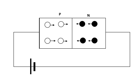
When a PN junction is formed without any external voltage (unbiased condition), a depletion layer and a potential barrier naturally develop. These play a crucial role in the behavior of semiconductor devices like diodes and transistors.
o A P-type semiconductor has an excess of holes (positive charge carriers).
o An N-type semiconductor has an excess of electrons (negative charge carriers).
o When the P-type and N-type materials are joined, some free electrons from the N-region move across the junction and recombine with holes in the P-region.
o Similarly, some holes from the P-region diffuse into the N-region and recombine with electrons.
o As electrons leave the N-region, they expose positive donor ions.
o As holes leave the P-region, they expose negative acceptor ions.
o This creates a region near the junction where there are no free charge carriers, only immobile positive and negative ions.
o This region is called the depletion layer because it is depleted of mobile charge carriers.
o The immobile ions in the depletion layer create an electric field pointing from the N-region to the P-region.
o This electric field opposes further movement of charge carriers across the junction.
o The electric field creates a potential barrier that prevents additional electrons from freely moving into the P-region and holes into the N-region.
o This built-in potential (also called the junction voltage) is typically:
| Property | Description |
|---|---|
| Depletion Layer | A region around the PN junction where there are no free charge carriers, only fixed positive and negative ions. |
| Potential Barrier | The electric potential that prevents further movement of charge carriers across the junction. |
| Thickness of Depletion Layer | Depends on the doping level—higher doping = thinner depletion layer. |
| Effect of Temperature | Higher temperature increases charge carrier generation, slightly reducing the barrier. |
• The PN junction diode does not conduct electricity in the unbiased state because of the potential barrier.
• However, when a forward voltage is applied, the barrier is reduced, allowing current to flow.
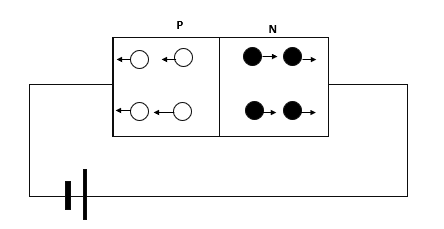
A PN junction can be biased in two ways: forward bias (allowing current to flow) and reverse bias (blocking current). The behavior of the junction in these conditions affects the current, depletion region, and barrier potential.
Forward bias means connecting the P-side to the positive terminal and the N-side to the negative terminal of a power supply.
| Property | Effect in Forward Bias |
|---|---|
| Current | A large current flows as electrons from the N-region and holes from the P-region move towards the junction and recombine. |
| Depletion Region | The depletion layer becomes narrower as more charge carriers (electrons and holes) move across the junction. |
| Barrier Potential | The potential barrier is reduced (from ~0.7V in silicon to near 0V), allowing charge carriers to flow easily. |
• The arrow points in the direction of current flow.
• Current flows easily in this direction.
Reverse bias means connecting the P-side to the negative terminal and the N-side to the positive terminal of a power supply.
| Property | Effect in Reverse Bias |
|---|---|
| Current | Almost no current flows (except for a tiny leakage current due to minority carriers). |
| Depletion Region | The depletion layer becomes wider as the majority carriers are pulled away from the junction. |
| Barrier Potential | The potential barrier is increased, making it harder for charge carriers to move across the junction. |
• The arrow opposes the applied voltage, meaning no significant current flows.
• Forward Bias: Used in LEDs, rectifier circuits, and voltage regulators to allow current flow.
• Reverse Bias: Used in Zener diodes, photodiodes, and voltage protection circuits to block or control current.
In reverse bias, a PN junction is connected with:
This causes the majority charge carriers (electrons in N-type and holes in P-type) to move away from the junction, making the depletion layer wider and the potential barrier higher. As a result, the junction strongly resists current flow.
However, a small leakage current still flows due to minority charge carriers.
o In the P-region, the minority carriers are free electrons (from thermal excitation).
o In the N-region, the minority carriers are holes.
o These minority carriers exist naturally due to thermal energy in the semiconductor.
o When a reverse bias is applied, minority carriers move in the opposite direction of majority carriers.
o Electrons in the P-region are attracted to the positive terminal.
o Holes in the N-region are attracted to the negative terminal.
o Since there are very few minority carriers, the resulting reverse current is extremely small.
o This small movement of minority carriers creates a very weak current (called reverse saturation current, 𝐼𝑠)
o In pure semiconductors, this current is almost negligible.
o In high-temperature conditions, more minority carriers are generated, increasing leakage current.
o This is why semiconductor devices fail at extremely high temperatures—they cannot fully block reverse current.
o If the reverse voltage is increased too much, two effects can occur:
| Factor | Effect on Reverse Current |
|---|---|
| Minority Carrier Concentration | More minority carriers = More leakage current. |
| Temperature | Higher temperature increases minority carriers, leading to higher leakage current. |
| Reverse Voltage | Small reverse voltage → Only leakage current flows. Large reverse voltage → Possible breakdown (Zener or Avalanche). |
• Reverse leakage current is usually undesirable in normal diodes, but in Zener diodes, it is used for voltage regulation.
Temperature has a significant impact on the behaviour of a PN junction diode, affecting both forward current (when the diode conducts) and reverse current (when the diode blocks current).
Forward Bias: The P-side is connected to the positive terminal, and the N-side is connected to the negative terminal, allowing current to flow.
• When temperature increases, more electrons in the valence band gain energy and move to the conduction band.
• This increases the number of charge carriers (electrons and holes), leading to higher current flow at the same applied voltage.
• The barrier potential (built-in voltage) decreases with temperature.
• For silicon diodes, the threshold voltage reduces by about 2.5mV per °C (e.g., from 0.7V to ~0.65V at higher temperatures).
• Since resistance decreases with temperature, the diode becomes more efficient in conducting current in forward bias.
Reverse Bias: The P-side is connected to the negative terminal, and the N-side is connected to the positive terminal, preventing current flow (except for a small leakage current).
• Minority charge carriers (electrons in the P-region and holes in the N-region) increase due to thermal generation.
• This results in a higher leakage current, even though the diode is supposed to block current.
• If temperature continues to rise, leakage current can become very large, leading to thermal runaway and diode failure.
• In Zener and Avalanche breakdown, high temperature worsens the effect, making the diode less reliable.
| Bias Type | Effect of Increasing Temperature |
|---|---|
| Forward Bias | Increases forward current (more charge carriers). Lowers threshold voltage (better conductivity) |
| Reverse Bias | Increases leakage current (more minority carriers). Risk of breakdown and diode failure |
• In power electronics, diodes must be cooled using heat sinks to prevent overheating.
• Temperature compensation circuits are used in precision circuits to counteract temperature effects.
When a PN junction diode is reverse biased, it ideally blocks current except for a tiny leakage current. However, if the reverse voltage is increased beyond a certain limit, the diode experiences breakdown, allowing a large reverse current to flow.
The two main types of breakdown are:
Occurs in highly doped diodes at low reverse voltages (~5V or less).
• When the reverse voltage reaches the Zener breakdown voltage, the electric field in the depletion region becomes extremely strong.
• This field is so strong that it pulls electrons from covalent bonds in the valence band, freeing them into the conduction band.
• This sudden increase in free electrons causes a sharp rise in reverse current.
• Zener diodes are used in power supplies to maintain a stable voltage despite changes in input voltage or load current.
Occurs in lightly doped diodes at high reverse voltages (above ~6V).
• As the reverse voltage increases, minority charge carriers in the depletion region gain high kinetic energy from the strong electric field.
• These fast-moving carriers collide with atoms, knocking off more electrons, creating a chain reaction called impact ionization.
• This multiplication of carriers leads to a sudden and uncontrollable increase in reverse current.
• Avalanche diodes are used in surge protectors to prevent damage from voltage spikes.
| Feature | Zener Breakdown | Avalanche Breakdown |
|---|---|---|
| Doping Level | Highly doped | Lightly doped |
| Depletion Layer | Narrow | Wide |
| Voltage Range | Low (2V–5V) | High (6V–50V) |
| Cause of Breakdown | Strong electric field pulling electrons from atoms | Carrier collisions causing impact ionization |
| Current Control | Controlled and stable | Rapid and uncontrollable if not managed |
| Application | Voltage regulation (Zener diodes) | High-voltage protection (Avalanche diodes) |
The current-voltage (I-V) curve of a diode is a graph that shows how the current through the diode varies with the voltage applied across it. The diode operates in three different regions based on the voltage applied:
• Description: When a positive voltage is applied across the diode (with the anode connected to the positive terminal and the cathode to the negative terminal), the diode is said to be in forward bias.
• For the diode to conduct, the forward voltage ( Vf ) must exceed a minimum threshold (usually 0.7V for silicon diodes).
• Behavior: In this region, the current increases exponentially as the voltage increases beyond the threshold.
• Graph: The I-V curve in the forward bias region rises steeply after the threshold voltage.
• Description: When the negative voltage is applied across the diode (with the anode connected to the negative terminal and the cathode to the positive terminal), the diode is in reverse bias.
• In reverse bias, current does not flow, except for a very small current called reverse saturation current (Is).
• Behavior: The diode behaves like an open circuit, showing high resistance to the flow of current in the reverse direction. The reverse saturation current is typically very small, but it still exists.
• Graph: The I-V curve is flat in the reverse bias region, showing a very small current.
• Description: When a large negative voltage is applied across the diode, it enters the breakdown region. This occurs when the reverse voltage exceeds the breakdown voltage (Vbr).
• Behavior: In this region, the diode allows current to flow in the reverse direction from cathode to anode. The current increases sharply in reverse, and the diode conducts in the reverse direction.
• Graph: The I-V curve steeply rises in the negative voltage range, indicating high reverse current once breakdown voltage is reached.
The characteristic graph can be visualized as follows:
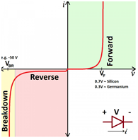
• 𝑉𝑡ℎ: Forward threshold voltage (typically 0.7V for silicon).
• 𝑉𝑏𝑟: Breakdown voltage.
• The curve shows exponential rise in forward bias (after the threshold) and nearly zero current in reverse bias (except for a small leakage current).
| Region | Voltage Applied | Current Behavior |
|---|---|---|
| Forward Bias | Positive (exceeds Vth) | Current increases exponentially after threshold. |
| Reverse Bias | Negative (less than Vth) | Very small current (reverse saturation current). |
| Breakdown Region | Large negative voltage | Large reverse current (after breakdown voltage, Vbr). |
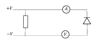
• The positive terminal of the battery is connected to the anode of the diode, and the negative terminal to the cathode.
• The diode faces forward, allowing current to flow through it easily
• Components Needed:
✅ PN Diode (e.g., 1N4148 for silicon)
✅ Variable DC Power Supply
✅ Resistor (to limit current)
✅ Ammeter (to measure current)
✅ Voltmeter (to measure diode voltage)
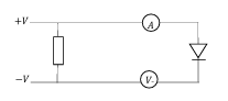
• The ammeter (𝐀) measures current (𝐼) through the diode.
• The voltmeter (𝐕) measures voltage (𝑉) across the diode.
• As voltage increases, the current rises exponentially after the threshold voltage.
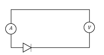
• Similar setup, but with the diode reversed:
The negative terminal of the battery is connected to the anode of the diode, and the positive terminal to the cathode.
The diode faces backward, blocking most of the current, except for a small leakage current in ideal conditions.
The static characteristics of a diode describe the relationship between the current flowing through the diode and the voltage applied across it. These characteristics are typically represented by the current-voltage (𝐼 − 𝑉) curve of the diode. The temperature has a significant effect on the behavior of the diode, particularly its forward voltage (𝑉𝑓) and the reverse saturation current (𝐼𝑠).
• As temperature increases:
o The forward voltage (𝑉𝑓) required to turn on the diode decreases. This means that as the temperature rises, the diode will start to conduct at a lower voltage.
o Reason: The thermal energy increases as temperature rises, which results in more charge carriers being available in the semiconductor material. This reduces the energy needed to overcome the barrier potential of the diode.
• Typical behavior:
o For a silicon diode, the forward voltage decreases by approximately −2.5 𝑚𝑉/°𝐶 for every degree Celsius increase in temperature.
• Effect on 𝐼 − 𝑉 curve:
o At higher temperatures, the 𝐼 − 𝑉 curve shifts to the left, meaning the diode will conduct more current at a lower voltage.
• As temperature increases:
o The reverse saturation current (𝐼𝑠) increases significantly. This is the very small current that flows in reverse bias (before the breakdown voltage is reached).
o Reason: The number of thermally generated charge carriers increases with temperature. This results in a higher reverse saturation current, as more minority carriers are available to contribute to the current flow in reverse bias.
• Typical behavior:
o For a silicon diode, the reverse saturation current doubles for every 10°𝐶 increase in temperature.
• Effect on 𝐼 − 𝑉 curve:
o As the reverse saturation current increases, the reverse current in the I-V curve will also increase at a higher temperature. This means that the diode will leak more current when reverse-biased at higher temperatures.
• As temperature increases:
o The reverse breakdown voltage (𝑉𝑏𝑟) decreases slightly. This is the voltage at which the diode starts to conduct heavily in reverse (in breakdown region).
o Reason: At higher temperatures, the semiconductor material becomes more conductive, and the breakdown voltage is reached at a lower reverse voltage.
• At higher temperatures:
o The diode conducts more current at lower voltages in forward bias, making it more sensitive and potentially leading to thermal runaway if not properly regulated.
o In reverse bias, the diode will exhibit an increased reverse leakage current and a slightly reduced breakdown voltage.
• Forward Voltage (𝑉𝑓): Decreases with an increase in temperature.
• Reverse Saturation Current (𝐼𝑠): Increases exponentially with temperature.
• Reverse Breakdown Voltage (𝑉𝑏𝑟): Slightly decreases with increasing temperature.
• At room temperature (around 25°𝐶), a silicon diode might have a forward voltage of about 0.7𝑉. If the temperature increases to 50°𝐶, the forward voltage might drop to around 0.68𝑉.
• The reverse saturation current, which is typically very small at room temperature (nano-amps), might increase to 𝑚𝑖𝑐𝑟𝑜 − 𝑎𝑚𝑝𝑠 at higher temperatures.
Power dissipation (𝑃𝑑) in a diode refers to the energy lost in the form of heat when current flows through the diode. This loss occurs because the diode has some forward voltage drop (𝑉𝑓), and when current (If) flows through it, energy is dissipated as heat.
The formula for power dissipation in a diode is:
𝑃𝑑 = 𝑉𝑓 × 𝐼𝑓
Where:
If a diode has a forward voltage drop of 0.7𝑉 and a forward current of 20𝑚𝐴 (0.02𝐴):
𝑃𝑑 = 0.7𝑉 × 0.02𝐴 = 0.014𝑊 (14 𝑚𝑊)
The maximum forward voltage (𝑉𝑓_𝑚𝑎𝑥) is the highest voltage that can be applied across the diode in the forward bias direction without damaging the diode. Exceeding this voltage can lead to thermal runaway or breakdown, damaging the diode permanently.
For typical silicon diodes, the forward voltage increases slightly with increasing current but should not exceed certain values for safe operation.𝑉𝑓_𝑚𝑎𝑥 is typically specified in the diode's datasheet.
A typical silicon diode might have a maximum forward voltage of 1.0V when operating at a higher current (e.g., 1A). Exceeding this can cause damage.
The maximum forward current (𝐼𝑓𝑚𝑎𝑥) is the highest amount of current that a diode can safely carry in the forward bias direction. If the current exceeds 𝐼𝑓𝑚𝑎𝑥 the diode can overheat and possibly be destroyed.
𝐼𝑓𝑚𝑎𝑥 typically specified in the diode's datasheet and depends on the diode's material, construction, and heat dissipation capacity.
If a diode has a maximum forward current rating of 1𝐴, and the current exceeds this value, it could damage the diode due to excessive heat generation.
Peak Inverse Voltage (𝑃𝐼𝑉), also known as the Reverse Breakdown Voltage (𝑉𝑅), is the maximum reverse voltage that a diode can withstand without breaking down and allowing large amounts of current to flow in the reverse direction. Exceeding this voltage can lead to reverse breakdown, where the diode might permanently conduct in reverse, potentially causing damage.
For silicon diodes, the 𝑃𝐼𝑉 is usually quite high, but this depends on the specific diode's rating.
If a reverse current flows in the diode during breakdown, power dissipation in reverse can be calculated using:
𝑃𝑑𝑟𝑒𝑣𝑒𝑟𝑠𝑒 = 𝑉𝑅 × 𝐼𝑟𝑒𝑣𝑒𝑟𝑠𝑒
Where:
Consider a diode with a 𝑃𝐼𝑉 of 100𝑉 and a reverse leakage current of 1mA (0.001𝐴):
𝑃𝑑𝑟𝑒𝑣𝑒𝑟𝑠𝑒 = 100𝑉 × 0.001𝐴 = 0.1𝑊
This represents the power dissipated in the reverse condition, and if the diode continues to operate at this condition for too long, it can overheat.
These parameters are essential in selecting a diode for specific applications to ensure it operates within safe limits and does not get damaged due to excessive power dissipation or reverse voltage breakdown.
An ideal diode is a theoretical diode that has no resistance when forward biased and completely blocks current when reverse biased. It has a perfect performance, meaning there is no voltage drop across it when conducting, and it does not allow any current to flow when reverse biased (no leakage current).
• Forward Bias (ON state): The diode acts as a perfect conductor (i.e., no resistance).
• Reverse Bias (OFF state): The diode acts as an open circuit (i.e., no current flows).
In Forward Bias: The diode behaves as a short circuit (zero voltage drop), and current flows freely.
• In Reverse Bias: The diode behaves as an open circuit (no current flows).
In real-world scenarios, a diode's forward voltage is not zero but is constant for a given current once the diode is conducting. This is an approximation commonly used in circuit analysis, where we assume a constant forward voltage drop (𝑉𝐷), such as 0.7𝑉 for silicon diodes.
• In the forward bias, the diode is modeled as a voltage source (V_D) in series with a small resistance (R_D) to account for the small resistance of the diode when conducting.
Where:
• 𝑉𝐷 is the constant forward voltage drop across the diode when it is conducting.
• 𝑅𝐷 is the small resistance of the diode when conducting, which is often neglected in ideal cases but can be considered in some real-world approximations.
o When the applied voltage exceeds 𝑉𝐷 (e.g., 0.7V for silicon), the diode starts to conduct.
o The voltage across the diode stays at 𝑉𝐷, and the current increases exponentially with the applied voltage.
o For small voltages below the forward voltage, the current is almost zero (very low leakage current).
o Above V_D, the diode conducts and the current increases sharply as the voltage increases.
Graph (I-V characteristic for a diode with constant forward voltage drop):
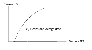
o When the diode is reverse biased, the current is negligible (ideally zero) until the breakdown voltage is reached.
o Reverse current (leakage current) is typically very small, and if the reverse voltage exceeds the breakdown voltage, the diode will enter the breakdown region.
Rectification is the process of converting Alternating Current (AC) into Direct Current (DC). This is necessary because many electronic devices operate on DC power, while electricity from power grids is in AC form. Diodes are used in rectifiers because they allow current to flow in only one direction.
• A single diode is used to allow only one half-cycle (positive or negative) of AC to pass through.
• The output is pulsating DC, meaning there are gaps in the current flow.
• Efficiency is low, making it suitable for simple applications like signal demodulation.
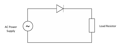
• During the positive half-cycle, the diode is forward biased, allowing current to pass through.
• During the negative half-cycle, the diode is reverse biased, blocking current flow.
• The result is a pulsating DC voltage output (only positive cycles appear).
• Uses four diodes in a bridge rectifier configuration or two diodes with a center-tap transformer to convert the entire AC waveform into DC.
• Produces a smoother output than half-wave rectification.
• More efficient and commonly used in DC power supplies.
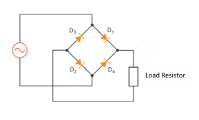
Load Resistor
• During the positive half-cycle, two diodes conduct and direct current in one direction through the load.
• During the negative half-cycle, the other two diodes conduct and direct current in the same direction through the load.
• The output is pulsating DC, but without gaps, making it easier to filter into steady DC.
• More efficient than half-wave rectification.
• Higher average output voltage.
• Less ripple, making it easier to filter.
Diodes can fail due to various reasons such as overheating, excessive current, or voltage stress. Here are the common diode faults:
• The diode fails and does not conduct at all, even when forward biased.
• Symptoms: No current flow in the circuit, leading to a complete failure of rectification.
• Cause: Overheating, manufacturing defects, or mechanical damage.
• The diode allows current to flow in both directions (forward and reverse), losing its rectification property.
• Symptoms: Excessive current flows through the circuit, potentially damaging other components.
• Cause: High voltage surges or excessive current.
• A small amount of current flows in reverse bias, which is normally blocked.
• Symptoms: Reduced efficiency of rectification.
• Cause: Aging of the diode or minor internal defects.
• The diode fails due to excessive reverse voltage, causing it to conduct in reverse bias.
• Symptoms: The diode no longer blocks reverse current, leading to circuit failure.
• Cause: Exceeding the diode’s Peak Inverse Voltage (PIV).
Testing a diode ensures that it is functioning correctly. The most common way to test a diode is by using a multimeter in Diode Mode or Resistance Mode.
| Condition | Expected Reading (Diode Mode) | Expected Reading (Resistance Mode) |
|---|---|---|
| Good Diode (Forward Bias) | 0.6V - 0.7V | Low Resistance (Ω) |
| Good Diode (Reverse Bias) | OL (No reading) | High Resistance (MΩ) |
| Open Diode | OL (Both directions) | High Resistance (Both directions) |
| Shorted Diode | 0V (Both directions) | Low Resistance (Both directions) |
Rectification is the conversion of AC to DC using diodes. Half-wave rectification uses one diode, while full-wave rectification (bridge rectifier) uses four diodes.
Diode faults include open circuit, short circuit, leakage current, and breakdown.
Testing diodes involves using a multimeter in diode mode to check for a voltage drop in forward bias and OL (no conduction) in reverse bias.
Opto-electronic devices are semiconductor components that either generate or respond to light. They convert electrical energy into light (light-emitting devices) or light into electrical energy (light-sensing devices). These devices are widely used in communication, sensing, display technology, and automation.
- Converts electrical energy into visible or infrared light.
- Made from semiconductor materials like Gallium Arsenide (GaAs) or Gallium Phosphide (GaP).
• When a forward voltage is applied to the LED, electrons and holes recombine at the PN junction.
• This recombination releases energy in the form of photons (light emission).
• The wavelength (color) of the light depends on the semiconductor material.
• Similar to an LED but produces a coherent, high-intensity light beam.
• Used in applications requiring precise and focused light.
• A strong forward bias causes electron-hole recombination, producing light.
• Mirrors inside the diode amplify the light, creating a laser beam.
• A light-sensitive diode that converts light into an electric current.
• Works in reverse bias mode, meaning it conducts only when exposed to light.
• When light photons hit the depletion region of the photodiode, they generate electron-hole pairs.
• These charge carriers increase the current flow in the circuit.
• More light = More current.
• A phototransistor is a light-sensitive transistor that acts like a photodiode but with higher sensitivity.
• Uses a transistor’s amplification property to detect even weak light signals.
• Light falling on the base-emitter junction generates charge carriers.
• This increases the base current, turning the transistor ON and allowing a large collector current to flow.
• Electrically isolates two circuits while allowing signal transmission through light.
• Consists of an LED and a photodetector (photodiode or phototransistor) enclosed in a single package.
• The LED emits light when an input signal is applied.
• The photodetector receives the light and converts it back into an electrical signal.
• No direct electrical connection between input and output, providing isolation.
• Converts sunlight into electrical energy (DC power).
• Made from silicon-based semiconductors.
• Light photons hit the PN junction, generating electron-hole pairs.
• The built-in electric field separates the charges, producing a voltage across the terminals.
• This produces a continuous DC current when exposed to light.
| Device | Function | Works On | Example Application |
|---|---|---|---|
| LED | Emits visible light | Forward Bias | TV screens, Indicators |
| Laser Diode | Emits focused laser beam | Forward Bias | Barcode scanners, CDs |
| Photodiode | Converts light to current | Reverse Bias | Light sensors, Cameras |
| Phototransistor | Light-sensitive transistor | Reverse Bias | IR remote sensors |
| Optocoupler | Isolates circuits via light | LED & Photodiode | Power electronics |
| Solar Cell | Converts light into power | Light Energy | Solar panels |
Optoelectronic devices are semiconductor components that either generate or detect light. They play a crucial role in various applications, including sensing, communication, and display technologies. Below, we describe the basic construction, operation, characteristics, and applications of:
✔ Made from a light-sensitive semiconductor material, such as cadmium sulfide (CdS) or cadmium selenide (CdSe).
✔ Two metal electrodes are placed on opposite sides of the semiconductor, forming electrical contacts.
✔ A transparent protective coating is applied to prevent damage.
• The resistance of an LDR decreases when exposed to light and increases in darkness.
• This happens because light energy excites electrons in the semiconductor, increasing conductivity.
• More light → More free electrons → Lower resistance → Higher current flow.
• Less light → Fewer free electrons → Higher resistance → Lower current flow.
✔ High resistance in the dark (Mega-ohms range).
✔ Low resistance in bright light (hundreds of ohms).
✔ Slow response time (not suitable for high-speed applications).
✔ Automatic streetlights (turn ON at night, OFF during the day).
✔ Camera light meters (detect ambient light levels).
✔ Solar-powered devices (adjust brightness based on light levels).
✔ Security alarms (detect shadows or movements).
✔ A PN junction diode made from silicon or germanium.
✔ It has a transparent window or lens to allow light to reach the depletion region.
✔ Operates mainly in reverse bias mode.
• When light strikes the depletion region, it creates electron-hole pairs.
• These charge carriers increase the reverse current in the diode.
• The higher the light intensity, the higher the current.
• Used mainly for light detection and optical communication.
✔ Works in reverse bias mode.
✔ Fast response time (suitable for high-speed applications).
✔ Very low dark current (minimal leakage current in darkness).
✔ Highly sensitive to infrared (IR) light.
✔ Optical communication (fiber optics, IR sensors, remote controls).
✔ Light sensors (automatic lighting, camera exposure control).
✔ Smoke detectors (detects scattered light from smoke particles).
✔ Medical instruments (pulse oximeters, blood oxygen sensors).
✔ A PN junction diode made from Gallium-based materials (GaAs, GaN, GaP).
✔ Encased in a transparent plastic dome for light dispersion.
✔ The anode (positive) and cathode (negative) terminals provide electrical connections.
•When forward biased, electrons move from the N-region to the P-region.
•They recombine with holes, releasing energy in the form of photons (light emission).
•The color of the emitted light depends on the bandgap energy of the semiconductor.
✔ Operates in forward bias.
✔ Low power consumption and high efficiency.
✔ Available in different colors (red, green, blue, white, etc.).
✔ Very fast switching speed (used in optical communication).
✔ Display screens (LED TVs, computer monitors, traffic lights).
✔ Indicator lights (power ON/OFF indicators in devices).
✔ Automotive lighting (headlights, brake lights, dashboard displays).
✔ Optical fiber communication (high-speed data transmission).
| Device | Construction | Operation | Characteristics | Applications |
|---|---|---|---|---|
| LDR (Photoconductive Cell) | Light-sensitive resistor (CdS) | Resistance decreases with light | Slow response, high resistance in the dark | Automatic lights, security systems |
| Photodiode | PN junction diode | Converts light into current | Works in reverse bias, fast response | Optical communication, light sensors |
| LED | PN junction diode (GaAs, GaP) | Converts electricity into light | Works in forward bias, efficient | Displays, indicators, lighting |
A transistor is a semiconductor device used for amplification and switching in electronic circuits. The most common type is the Bipolar Junction Transistor (BJT), which consists of three layers of semiconductor material and operates using both electrons and holes as charge carriers.
BJTs come in two types:
• ✔ NPN transistor – Current flows from collector to emitter when forward biased.
• ✔ PNP transistor – Current flows from emitter to collector when forward biased.1
Each transistor has three terminals:
• Emitter (E) – Releases charge carriers.
• Base (B) – Controls the transistor operation.
• Collector (C) – Collects charge carriers.2
• ✔ A small current at the base controls a larger current between the collector and emitter.
• ✔ The transistor acts as a current amplifier or a switch.
• ✔ Has two N-type semiconductor layers separated by a P-type base.4
• ✔ The collector (C) and emitter (E) are N-type, and the base (B) is P-type.
• ✔ Operates when the base-emitter junction is forward biased and the base-collector junction is reverse biased.
• A small current is applied at the base.
• This allows electrons to flow from emitter to collector.
• The transistor is ON and conducts current from collector to emitter.
• Base-Emitter Junction (V_BE) → Forward biased (+0.7V for silicon, +0.3V for germanium).
• Collector-Base Junction (V_CB) → Reverse biased (higher voltage at collector).
• ✔ Has two P-type semiconductor layers separated by an N-type base.
• ✔ The collector (C) and emitter (E) are P-type, and the base (B) is N-type.
• ✔ Operates when the base-emitter junction is forward biased and the base-collector junction is reverse biased.
• A small current is applied at the base (negative with respect to emitter).5
• This allows holes to flow from emitter to collector.
The transistor is ON and conducts current from emitter to collector.
• Base-Emitter Junction (V_BE) → Forward biased (-0.7V for silicon, -0.3V for germanium).
• Collector-Base Junction (V_CB) → Reverse biased (higher voltage at emitter).
A transistor can be connected in three different configurations:
• ✔ Base is common to both input and output.6
• ✔ Input: Applied between emitter and base.
• ✔ Output: Taken from collector and base.
• ✔ Current gain (α) is less than 1 (low gain).
• ✔ High-frequency amplifiers.
• ✔ Emitter is common to both input and output.
• ✔ Input: Applied between base and emitter.
• ✔ Output: Taken from collector and emitter.
• ✔ Current gain (β) is high (20-200).
• ✔ Most widely used for signal amplification.
• ✔ Collector is common to both input and output.
• ✔ Input: Applied between base and collector.
• ✔ Output: Taken from emitter and collector.
• ✔ Voltage gain is less than 1, but current gain is high.
• ✔ Used as a buffer for impedance matching.
| Configuration | Input | Output | Gain | Applications |
|---|---|---|---|---|
| Common Base (CB) | Emitter-Base | Collector-Base | Low | High-frequency amplifiers |
| Common Emitter (CE) | Base-Emitter | Collector-Emitter | High | General signal amplification |
| Common Collector (CC) | Base-Collector | Emitter-Collector | Low (voltage), High (current) | Impedance matching |
• ✔ NPN transistors conduct when base is positive, while PNP transistors conduct when base is negative.7
• ✔ The base current controls the collector current, making the transistor act as an amplifier or switch.8
• ✔ Common Emitter (CE) is the most commonly used configuration for amplifiers.
Transistor parameters define the amplification capabilities of a transistor in terms of voltage gain and current gain. These are essential for understanding how transistors function as amplifiers and switches.
Definition: Voltage gain is the ratio of the output voltage to the input voltage in an amplifier circuit.9 It indicates how much a transistor amplifies the input signal voltage.
𝐴𝑣 = 𝑉𝑜𝑢𝑡 / 𝑉𝑖𝑛
Where:
• ✔ 𝐴𝑣 = Voltage gain
• ✔ 𝑉𝑜𝑢𝑡 = Output voltage
• ✔ 𝑉𝑖𝑛 = Input voltage
• ✔ A higher voltage gain means a stronger amplification of the input signal.
• ✔ Voltage gain is unitless because it is a ratio.
• ✔ In Common Emitter (CE) configuration, voltage gain is high.10
If an amplifier has an input voltage of 0.1V and an output voltage of 5V, the voltage gain is:
𝐴𝑣 = 5𝑉 / 0.1𝑉 = 50
This means the transistor amplifies the input voltage 50 times.
Current gain measures how much the transistor amplifies the input current. There are two important current gain parameters:
• ✔ Symbol: 𝛽 (Beta)
• ✔ Definition: Ratio of collector current (𝐼𝐶) to base current (𝐼𝐵).β = 𝐼𝐶 / 𝐼𝐵
• ✔ Typically ranges between 20 to 500 for most BJTs.
• ✔ A higher β means the transistor is more efficient at amplifying current.
If the base current is 0.5mA and the collector current is 50mA, then:
β = 50𝑚𝐴 / 0.5𝑚𝐴 = 100
This means the transistor amplifies the base current 100 times.
• ✔ Symbol: 𝛼 (Alpha)
• ✔ Definition: Ratio of collector current (IC) to emitter current (𝐼𝐸).𝛼 = 𝐼𝐶 / 𝐼𝐸
• ✔ α is always less than 1, typically between 0.95 to 0.99.
• ✔ α and β are related by: 𝛼 = 𝛽 / (𝛽 + 1)
Voltage gain and current gain are related in amplifier circuits. The power gain is the product of voltage and current gain:
𝑃𝑜𝑤𝑒𝑟 𝐺𝑎𝑖𝑛 = 𝐴𝑣 × 𝛽
• ✔ Voltage gain (Av) measures how much the transistor amplifies voltage.13
• ✔ Current gain (β and α) measures how much the transistor amplifies current.14
• ✔ Common Emitter (CE) transistors are widely used for high voltage and current gain applications.15
A transistor switching circuit is a circuit where a transistor acts as an electronic switch to control current flow.16 The transistor operates in two modes:
• ✔ Cutoff Region (OFF state – no current flows).
• ✔ Saturation Region (ON state – full current flows).
These circuits are widely used in digital logic, motor control, and signal amplification.
A phototransistor is similar to a normal BJT (Bipolar Junction Transistor) but with a light-sensitive base.17 Instead of an electrical signal, it is activated by light.
• ✔ Structure:
o Usually an NPN transistor.
o Has three layers (Emitter, Base, Collector), but the Base is exposed to light instead of being electrically connected.
o Can be packaged in transparent casings to allow light to enter.
• ✔ When light falls on the base, it generates electron-hole pairs, causing current to flow from collector to emitter.
• ✔ More light intensity → More base current → More collector current (higher amplification).
• ✔ In dark conditions, the transistor is OFF (cutoff state).
• ✔ When light is present, the transistor switches ON (saturation state).
• ✔ Light detection and control (e.g., automatic streetlights).
• ✔ Optical switching (e.g., remote-control receivers).
• ✔ Security systems (e.g., motion sensors).
A Darlington Pair is a special transistor configuration where two BJTs are connected to work as a single unit.
• ✔ Structure:
o The emitter of the first transistor (T1) is connected to the base of the second transistor (T2).
o This provides high current gain (β).
• ✔ A small base current in T1 is amplified and passed to the base of T2.
• ✔ T2 further amplifies this current, resulting in a large collector current.
• ✔ Acts as a high-gain switch, needing only a small input signal to turn ON large loads.
βtotal = β1 × β2
• ✔ If β1 = 100 and β2 = 50, the total gain is:
βtotal = 100 × 50 = 5000
• ✔ High-power switching (e.g., controlling motors, relays, and LEDs).
• ✔ Sensor amplification (e.g., touch switches).
• ✔ Audio amplifiers (e.g., boosting weak signals).
A thyristor (or SCR - Silicon Controlled Rectifier) is a four-layer semiconductor switch made of PNPN structure.
• ✔ Structure:
o Has three terminals: Anode (A), Cathode (K), and Gate (G).
o Works like a diode but needs a trigger pulse at the gate to switch ON.
• ✔ OFF State (Blocking Mode):
o Without a gate pulse, the SCR remains OFF, blocking current flow.
• ✔ ON State (Conducting Mode):
o A small current at the gate (G) turns the SCR ON, allowing current to flow from anode to cathode.
o Once ON, the SCR remains conducting even if the gate signal is removed.
• ✔ Turning OFF:
o To switch OFF, the current must drop to zero (by removing power or using a commutation circuit).
• ✔ Power control (e.g., dimming lights, motor speed control).
• ✔ Rectifiers and inverters.
• ✔ Over-voltage protection (crowbar circuits).
| Component | Structure | Working Principle | Applications |
|---|---|---|---|
| Phototransistor | Light-sensitive BJT | Light triggers conduction amplification | Light sensors, remote controls |
| Darlington Pair | Two BJTs in series | High current gain amplification | High-power switching, touch switches |
| Thyristor (SCR) | PNPN structure | Requires gate pulse, stays ON after triggering | Power control, motor drives |
• ✔ Phototransistors work based on light activation instead of a base current.
• ✔ Darlington Pair transistors provide very high current gain, making them ideal for power switching.
• ✔ Thyristors (SCRs) need a gate pulse to turn ON and stay conducting until the current is removed.
Unipolar transistors are semiconductor devices that control current flow using only one type of charge carrier, either electrons or holes. Unlike Bipolar Junction Transistors (BJTs), which use both electrons and holes, unipolar transistors rely on an electric field to control conductivity.
Unipolar transistors are semiconductor devices that control current flow using only one type of charge carrier, either electrons or holes. Unlike Bipolar Junction Transistors (BJTs), which use both electrons and holes, unipolar transistors rely on an electric field to control conductivity.
There are two main types:
• Field-Effect Transistors (FETs)
o Junction Field-Effect Transistor (JFET)
o Metal-Oxide Semiconductor Field-Effect Transistor (MOSFET)
• ✔ Made of a semiconductor channel (N-type or P-type) with two junctions.
• ✔ Has three terminals:
o Gate (G) – Controls current flow.
o Source (S) – Current enters.
o Drain (D) – Current exits.
• ✔ When a voltage is applied to the gate (G), it creates an electric field that controls the current flow from Source (S) to Drain (D).
• ✔ No gate current is required (high input impedance).
• ✔ Types of JFETs:
o N-channel JFET → Current flows via electrons (faster).
o P-channel JFET → Current flows via holes (slower).
• ✔ Used in low-noise amplifiers and buffer circuits.
• ✔ Has four layers: Gate (G), Source (S), Drain (D), and Substrate (Body).
• ✔ The Gate (G) is separated from the channel by a thin oxide layer, making it highly sensitive to voltage.
• ✔ Types of MOSFETs:
o Enhancement Mode MOSFET (E-MOSFET) → Needs a positive voltage at the gate to turn ON.
o Depletion Mode MOSFET (D-MOSFET) → Conducts by default, but can be turned OFF by applying voltage.
• ✔ Applying voltage to the Gate (G) creates an electric field, forming a conductive channel between Source (S) and Drain (D).
• ✔ No gate current is needed (only voltage).
• ✔ Used in power amplifiers, microprocessors, and digital circuits.
| Feature | JFET | MOSFET |
|---|---|---|
| Control Method | Voltage-controlled | Voltage-controlled |
| Input Impedance | High | Very High |
| Power Consumption | Low | Lower |
| Speed | Moderate | Faster |
| Applications | Low-noise amplifiers | Power circuits, microprocessors |
The Junction Field-Effect Transistor (JFET) is a voltage-controlled unipolar transistor that controls current flow using an electric field. It has three terminals:
• ✔ Gate (G) – Controls current flow.
• ✔ Source (S) – Where current enters.
• ✔ Drain (D) – Where current exits.
• The current flows between the Source (S) and Drain (D) through a semiconductor channel (N-type or P-type).
• A voltage applied to the Gate (G) creates an electric field, which restricts or allows the flow of current.
• Unlike BJTs, JFETs do not require a gate current, making them energy efficient.
The current-voltage (I-V) characteristics of a JFET can be divided into three regions:
• ✔ At low drain-to-source voltage (VDS), the JFET behaves like a resistor, and current (ID) increases linearly with voltage.
• ✔ When the Gate-Source voltage (VGS) is negative, the channel narrows, reducing current flow.
• ✔ Current remains nearly constant, making JFET useful for amplification.
• ✔ When VGS is more negative than the pinch-off voltage (VP), the channel closes completely, and no current flows.
• ✔ The JFET is in the OFF state.
• ✔ Integrated Circuits (ICs) are miniature electronic circuits where multiple components like transistors, resistors, and capacitors are fabricated onto a single silicon chip.
• ✔ They enable fast processing, compact size, and low power consumption.
• ✔ Computers & Smartphones – Microprocessors and memory chips.
• ✔ Communication Systems – Wireless transmitters and receivers.
• ✔ Automobiles – Engine control units (ECUs) and sensors.
• ✔ Medical Devices – Pacemakers, hearing aids, and imaging systems.
Voltage gain and current gain are related in amplifier circuits. The power gain is the product of voltage and current gain:
𝑃𝑜𝑤𝑒𝑟 𝐺𝑎𝑖𝑛 = 𝐴𝑣 × 𝛽
• ✔ Voltage gain (Av) measures how much the transistor amplifies voltage.13
• ✔ Current gain (β and α) measures how much the transistor amplifies current.14
• ✔ Common Emitter (CE) transistors are widely used for high voltage and current gain applications.15
A transistor switching circuit is a circuit where a transistor acts as an electronic switch to control current flow.16 The transistor operates in two modes:
• ✔ Cutoff Region (OFF state – no current flows).
• ✔ Saturation Region (ON state – full current flows).
These circuits are widely used in digital logic, motor control, and signal amplification.
A phototransistor is similar to a normal BJT (Bipolar Junction Transistor) but with a light-sensitive base.17 Instead of an electrical signal, it is activated by light.
• ✔ Structure:
o Usually an NPN transistor.
o Has three layers (Emitter, Base, Collector), but the Base is exposed to light instead of being electrically connected.
o Can be packaged in transparent casings to allow light to enter.
• ✔ When light falls on the base, it generates electron-hole pairs, causing current to flow from collector to emitter.
• ✔ More light intensity → More base current → More collector current (higher amplification).
• ✔ In dark conditions, the transistor is OFF (cutoff state).
• ✔ When light is present, the transistor switches ON (saturation state).
• ✔ Light detection and control (e.g., automatic streetlights).
• ✔ Optical switching (e.g., remote-control receivers).
• ✔ Security systems (e.g., motion sensors).
A Darlington Pair is a special transistor configuration where two BJTs are connected to work as a single unit.
• ✔ Structure:
o The emitter of the first transistor (T1) is connected to the base of the second transistor (T2).
o This provides high current gain (β).
• ✔ A small base current in T1 is amplified and passed to the base of T2.
• ✔ T2 further amplifies this current, resulting in a large collector current.
• ✔ Acts as a high-gain switch, needing only a small input signal to turn ON large loads.
βtotal = β1 × β2
• ✔ If β1 = 100 and β2 = 50, the total gain is:
βtotal = 100 × 50 = 5000
• ✔ High-power switching (e.g., controlling motors, relays, and LEDs).
• ✔ Sensor amplification (e.g., touch switches).
• ✔ Audio amplifiers (e.g., boosting weak signals).
A thyristor (or SCR - Silicon Controlled Rectifier) is a four-layer semiconductor switch made of PNPN structure.
• ✔ Structure:
o Has three terminals: Anode (A), Cathode (K), and Gate (G).
o Works like a diode but needs a trigger pulse at the gate to switch ON.
• ✔ OFF State (Blocking Mode):
o Without a gate pulse, the SCR remains OFF, blocking current flow.
• ✔ ON State (Conducting Mode):
o A small current at the gate (G) turns the SCR ON, allowing current to flow from anode to cathode.
o Once ON, the SCR remains conducting even if the gate signal is removed.
• ✔ Turning OFF:
o To switch OFF, the current must drop to zero (by removing power or using a commutation circuit).
• ✔ Power control (e.g., dimming lights, motor speed control).
• ✔ Rectifiers and inverters.
• ✔ Over-voltage protection (crowbar circuits).
| Component | Structure | Working Principle | Applications |
|---|---|---|---|
| Phototransistor | Light-sensitive BJT | Light triggers conduction | Light sensors, remote controls |
| Darlington Pair | Two BJTs in series | High current gain amplification | High-power switching, touch switches |
| Thyristor (SCR) | PNPN structure | Requires gate pulse, stays ON after triggering | Power control, motor drives |
• ✔ Phototransistors work based on light activation instead of a base current.
• ✔ Darlington Pair transistors provide very high current gain, making them ideal for power switching.
• ✔ Thyristors (SCRs) need a gate pulse to turn ON and stay conducting until the current is removed.
Unipolar transistors are semiconductor devices that control current flow using only one type of charge carrier, either electrons or holes. Unlike Bipolar Junction Transistors (BJTs), which use both electrons and holes, unipolar transistors rely on an electric field to control conductivity.
Unipolar transistors are semiconductor devices that control current flow using only one type of charge carrier, either electrons or holes. Unlike Bipolar Junction Transistors (BJTs), which use both electrons and holes, unipolar transistors rely on an electric field to control conductivity.
There are two main types:
• Field-Effect Transistors (FETs)
o Junction Field-Effect Transistor (JFET)
o Metal-Oxide Semiconductor Field-Effect Transistor (MOSFET)
• ✔ Made of a semiconductor channel (N-type or P-type) with two junctions.
• ✔ Has three terminals:
o Gate (G) – Controls current flow.
o Source (S) – Current enters.
o Drain (D) – Current exits.
• ✔ When a voltage is applied to the gate (G), it creates an electric field that controls the current flow from Source (S) to Drain (D).
• ✔ No gate current is required (high input impedance).
• ✔ Types of JFETs:
o N-channel JFET → Current flows via electrons (faster).
o P-channel JFET → Current flows via holes (slower).
• ✔ Used in low-noise amplifiers and buffer circuits.
• ✔ Has four layers: Gate (G), Source (S), Drain (D), and Substrate (Body).
• ✔ The Gate (G) is separated from the channel by a thin oxide layer, making it highly sensitive to voltage.
• ✔ Types of MOSFETs:
o Enhancement Mode MOSFET (E-MOSFET) → Needs a positive voltage at the gate to turn ON.
o Depletion Mode MOSFET (D-MOSFET) → Conducts by default, but can be turned OFF by applying voltage.
• ✔ Applying voltage to the Gate (G) creates an electric field, forming a conductive channel between Source (S) and Drain (D).
• ✔ No gate current is needed (only voltage).
• ✔ Used in power amplifiers, microprocessors, and digital circuits.
| Feature | JFET | MOSFET |
|---|---|---|
| Control Method | Voltage-controlled | Voltage-controlled |
| Input Impedance | High | Very High |
| Power Consumption | Low | Lower |
| Speed | Moderate | Faster |
| Applications | Low-noise amplifiers | Power circuits, microprocessors |
The Junction Field-Effect Transistor (JFET) is a voltage-controlled unipolar transistor that controls current flow using an electric field. It has three terminals:
• ✔ Gate (G) – Controls current flow.
• ✔ Source (S) – Where current enters.
• ✔ Drain (D) – Where current exits.
• The current flows between the Source (S) and Drain (D) through a semiconductor channel (N-type or P-type).
• A voltage applied to the Gate (G) creates an electric field, which restricts or allows the flow of current.
• Unlike BJTs, JFETs do not require a gate current, making them energy efficient.
The current-voltage (I-V) characteristics of a JFET can be divided into three regions:
• ✔ At low drain-to-source voltage (VDS), the JFET behaves like a resistor, and current (ID) increases linearly with voltage.
• ✔ When the Gate-Source voltage (VGS) is negative, the channel narrows, reducing current flow.
• ✔ Current remains nearly constant, making JFET useful for amplification.
• ✔ When VGS is more negative than the pinch-off voltage (VP), the channel closes completely, and no current flows.
• ✔ The JFET is in the OFF state.
• ✔ Integrated Circuits (ICs) are miniature electronic circuits where multiple components like transistors, resistors, and capacitors are fabricated onto a single silicon chip.
• ✔ They enable fast processing, compact size, and low power consumption.
• ✔ Computers & Smartphones – Microprocessors and memory chips.
• ✔ Communication Systems – Wireless transmitters and receivers.
• ✔ Automobiles – Engine control units (ECUs) and sensors.
• ✔ Medical Devices – Pacemakers, hearing aids, and imaging systems.
Voltage gain and current gain are related in amplifier circuits. The power gain is the product of voltage and current gain:
𝑃𝑜𝑤𝑒𝑟 𝐺𝑎𝑖𝑛 = 𝐴𝑣 × 𝛽
• ✔ Voltage gain (Av) measures how much the transistor amplifies voltage.13
• ✔ Current gain (β and α) measures how much the transistor amplifies current.14
• ✔ Common Emitter (CE) transistors are widely used for high voltage and current gain applications.15
A transistor switching circuit is a circuit where a transistor acts as an electronic switch to control current flow.16 The transistor operates in two modes:
• ✔ Cutoff Region (OFF state – no current flows).
• ✔ Saturation Region (ON state – full current flows).
These circuits are widely used in digital logic, motor control, and signal amplification.